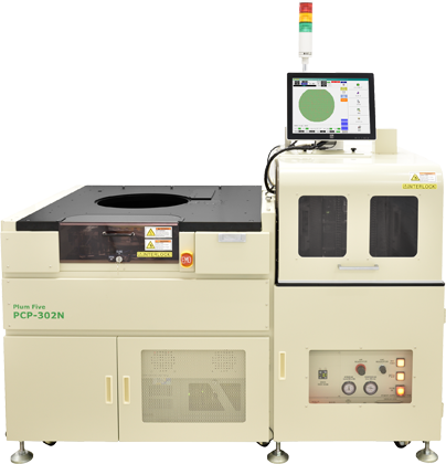
Top > Products > Wafer Prober > PCP-302N

Wafer Prober
PCP-302N


Outline

The PCP-302N is a wafer prober developed to respond to our customer's request flexibly on the basis of our experience and technology.
By adopting PFC original XY Compensation and Profiling function, PCP-302N can compensate the position even for the wafer's expansion caused by the temperature.


FEATURES

・ Effective compensation even for the wafer's expansion caused by the temperature.
・ Successful record of Alignment for customers' products is 100%. (Record only in Japan)
・ Probing more than two points by moving in a chip (Micro Probing)
・ Surface finish for your intended usage, such as gold plate, nickel plate, etc.
・ Low noise: More than -80dB on the chuck
 (Reference Value: 30KHZ to 30MHZ Loop ANT actual measurement)
・ High rigidity cabinet made by the iron surface plate and the welding frame realizes low vibration
・ Low cost and High throughput
・ Small space (Footprint), power-saving design
・ Stable operation (more than MTBF5000 hours)


OPTIONS

・ Supports chip probing by the wafer adapter.
・ Large diameter Pre-alignment chuck can handle a warped wafer, thin wafer and TAIKO™ Wafer
・ Quick Loader can reduce the Load/Unload time per sheet to half.
・ Capable of the high temperature range (50 ℃ to 150 ℃) and the precise thermal control (25℃±0.3℃).
※Reference value (standard system): Chuck surface: 0.04mT
                   Transporting rout: 0.2mT


SPECIFICATION

Wafer size 8 inch to 12 inch
Probing area Wafer: φ300mm
XY stage Driven by linear motor (Repeat accuracy:1um)
Footprint Small space: (W)1615mm × (D)1000mm


OTHERS

・ Total Sales of PCP Series: More than 500 sets (As of April 2025)
・ We can respond to the request from a customer flexibly.
・ We can offer discount for the purchase of several sets together.

 Products
for more information
Site Map | Terms of Use | Privacy Policy © Plum Five Co., Ltd.